Revealing the Crystalline Integrity of Wafer-Scale Graphene on SiO2/Si: An Azimuthal RHEED Approach

Abstract
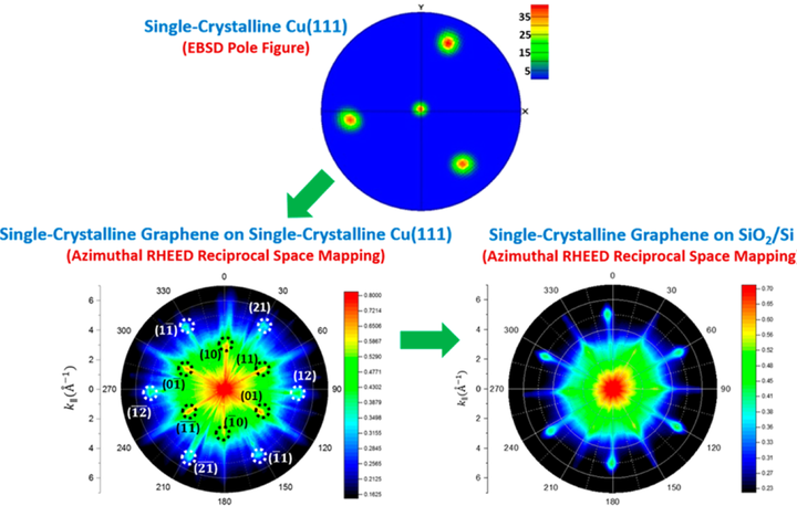
The symmetry of graphene is usually determined by a low-energy electron diffraction (LEED) method when the graphene is on the conductive substrates, but LEED cannot handle graphene transferred to SiO2/Si substrates due to the charging effect. While transmission electron microscopy can generate electron diffraction on post-transferred graphene, this method is too localized. Herein, we employed an azimuthal reflection high-energy electron diffraction (RHEED) method to construct the reciprocal space mapping and determine the symmetry of wafer-size graphene both pre- and post-transfer. In this work, single-crystalline Cu(111) films were prepared on sapphire(0001) and spinel(111) substrates with sputtering. Then the graphene was epitaxially grown on single-crystalline Cu(111) films with a low pressure chemical vapor deposition. The reciprocal space mapping using azimuthal RHEED confirmed that the graphene grown on Cu(111) films was single-crystalline, no matter the form of the monolayer or multilayer structure. While the Cu(111) film grown on sapphire(0001) may occasionally consist of 60° in-plane rotational twinning, the reciprocal space mapping revealed that the in-plane orientation of graphene grown atop was not affected. The proposed method for checking the crystalline integrity of the post-transferred graphene sheets is an important step in the realization of the graphene as a platform to fabricate electronic and optoelectronic devices.