van der Waals Epitaxy of Antimony Islands, Sheets, and Thin Films on Single-Crystalline Graphene

Abstract
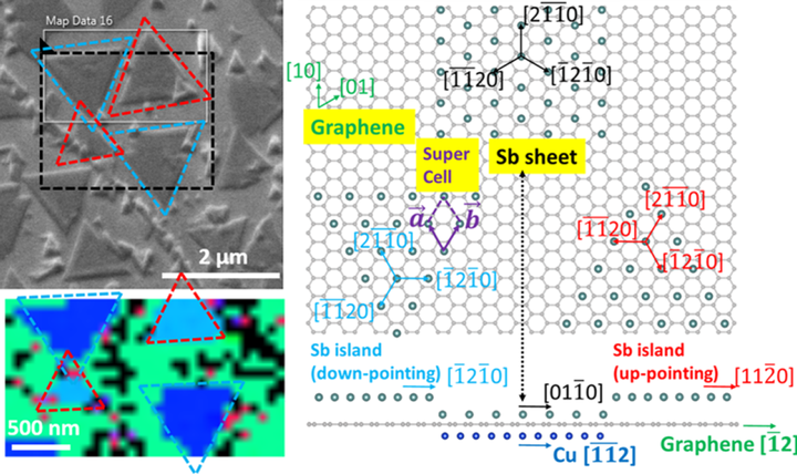
Antimony (Sb) nanostructures, including islands, sheets, and thin films, of high crystallinity were epitaxially grown on single-crystalline graphene through van der Waals interactions. Two types of graphene substrates grown by chemical vapor deposition were used, the as-grown graphene on Cu(111)/c-sapphire and the transferred graphene on SiO2/Si. On the as-grown graphene, deposition of ultrathin Sb resulted in two growth modes and associated morphologies of Sb. One was Sb islands grown in Volmer–Weber (VW) mode, and the other was Sb sheets grown in Frank–van der Merve (FM) mode. In contrast, only Sb islands grown in VW mode were found in a parallel growth experiment on the transferred graphene. The existence of Sb sheets on the as-grown graphene was attributed to the remote epitaxy between Sb and Cu underneath the graphene. In addition, Sb thin films were grown on both the as-grown and transferred graphene substrates. Both films indicated high quality, and no significant difference can be found between these two films. This work unveiled two epitaxial alignments between Sb(0001) and graphene, namely, Sb [101̅0]∥graphene [10] for Sb islands and Sb [21̅1̅0]∥graphene [10] for Sb sheets. For Sb thin films on graphene, the epitaxial alignment followed that of Sb islands, implying that Sb thin films originated from the continued growth of Sb islands. Last, Raman spectroscopy was used to probe the state of graphene under ultrathin Sb. No strain, doping, or disorder was found in the graphene postgrowth of Sb. The knowledge of the interface formation between ultrathin Sb and graphene provides a valuable foundation for future research on van der Waals heterostructures between antimonene and graphene.