Growth of epitaxial CdTe thin films on amorphous substrates using single crystal graphene buffer

Abstract
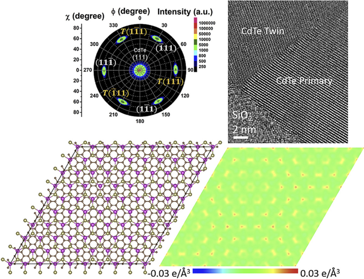
Traditionally, a high-quality CdTe film can only be grown on a single crystal substrate with a small lattice mismatch. Herein, we report the epitaxy of CdTe films on monolayer single crystal graphene buffered amorphous SiO2/Si(100) substrates, despite a 86% lattice mismatch between CdTe(111) and graphene. X-ray pole figure, electron backscatter diffraction mapping and transmission electron microscopy all confirm that the epitaxial CdTe films are composed of two domains: the primary and the Σ3 twin. The crystal quality of films is shown to improve as the post-deposition annealing temperature increases. However, the rotational misalignment in CdTe remains large even after annealing. Through density functional theory calculations on the charge transfer distribution at the interface of CdTe and graphene, it is found that the interface is dominated by the weak van der Waals interaction, which explains the large spread of in-plane orientation in CdTe films. Furthermore, the rotational misalignment in graphene itself is also confirmed to produce the large in-plane orientation spread in CdTe films. Although imperfect in epitaxy quality, this work demonstrates that monolayer single crystal graphene can buffer amorphous substrates for growing epitaxial films, and hence hints an opportunity for developing advanced thin film devices using graphene as a template.