Abstract
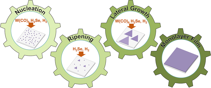
A multistep diffusion-mediated process was developed to control the nucleation density, size, and lateral growth rate of WSe2 domains on c-plane sapphire for the epitaxial growth of large area monolayer films by gas source chemical vapor deposition (CVD). The process consists of an initial nucleation step followed by an annealing period in H2Se to promote surface diffusion of tungsten-containing species to form oriented WSe2 islands with uniform size and controlled density. The growth conditions were then adjusted to suppress further nucleation and laterally grow the WSe2 islands to form a fully coalesced monolayer film in less than 1 h. Postgrowth structural characterization demonstrates that the WSe2 monolayers are single crystal and epitaxially oriented with respect to the sapphire and contain antiphase grain boundaries due to coalescence of 0° and 60° oriented WSe2 domains. The process also provides fundamental insights into the two-dimensional (2D) growth mechanism. For example, the evolution of domain size and cluster density with annealing time follows a 2D ripening process, enabling an estimate of the tungsten-species surface diffusivity. The lateral growth rate of domains was found to be relatively independent of substrate temperature over the range of 700–900 °C suggesting a mass transport limited process, however, the domain shape (triangular versus truncated triangular) varied with temperature over this same range due to local variations in the Se/W adatom ratio. The results provide an important step toward atomic level control of the epitaxial growth of WSe2 monolayers in a scalable process that is suitable for large area device fabrication.